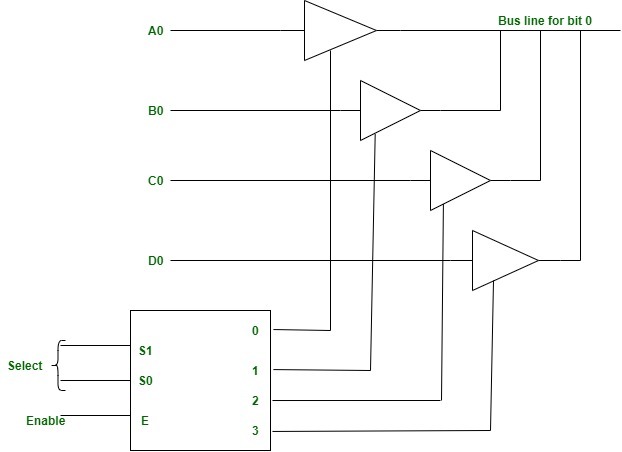
Q.1 (a) Explain three state buffers.
Tri-state buffer that means a buffer with three states and in that case two states are as usual one is input another is output with logic states either 0 or 1 but now we are adding one more state that is the third state named as high impedance state which makes the buffer gate to work as an open state circuit.

It contains both normal input and control input. Here, the output state is determined by the control input.
- When the control input is 1, the output is enabled and the gate will behave like a conventional buffer.
- When the control input is 0, the output is disabled and the gate will be in a high impedance state.
- To form a single bus line, all the outputs of the 4 buffers are connected together.
- The control input will now decide which of the 4 normal inputs will communicate with the bus line.
- The decoder is used to ensure that only one control input is active at a time.
- The diagram of a 3-state buffer can be seen below.
(b) Describe BUN and BSA memory reference instructions in detail.
BUN
The Branch Unconditionally (BUN) instruction can send the instruction that is determined by the effective address. They understand that the address of the next instruction to be performed is held by the PC and it should be incremented by one to receive the address of the next instruction in the sequence. If the control needs to implement multiple instructions that are not next in the sequence, it can execute the BUN instruction.
BSA
BSA stands for Branch and Save return Address. These instructions can branch a part of the program (known as subroutine or procedure). When this instruction is performed, BSA will store the address of the next instruction from the PC into a memory location that is determined by the effective address.
(c) What is interrupt? Describe interrupt cycle with neat diagram.
An interrupt is an event that alters the sequence in which the processor executes instructions.
Interrupt processing
instruction cycle consists of fetch, execute and interrupt stage show in below diagram −
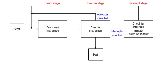
Interrupt handler activates most prior able activity first and later deferrable part will be handled.
Step 1 − First device issues interrupt to CPU.
Step 2 − Then, the CPU finishes execution of current instruction.
Step 3 − CPU tests for pending interrupt request. If there is one, it sends an acknowledgment to the device which removes its interrupt signal.
Step 4 − CPU saves program status word onto control stack.
Step 5 − CPU loads the location of the interrupt handler into the PC register.
Step 6 − Save the contents of all registers from the control stack into memory.
Step 7 − Find out the cause of interrupt, or interrupt type or invokes appropriate routine.
Step 8 − Restore saved registers from the stack.
Step 9 − Restore PC to dispatch the original process.
Q.2 (a) Differentiate assembly language and machine language.
Difference Between Machine Language and Assembly Language
| Parameters | Machine Language | Assembly Language |
| Nature of Syntax | The machine languages consist of 1s and 0s as binary digits. | The assembly languages have a similar syntax to that of the English language- thus making it easy for general users to understand (other than the programmers). |
| Ease of Comprehension | Only computers can comprehend machine languages. A normal human doesn’t possess the capacity to decipher it. | It is very easy for any human to understand, apply, and use assembly language. Machines cannot directly read and understand them. |
| Level of Language | The machine language is the lowest level of all the programming languages. It executes all the instructions directly through the CPU (Central Processing System) of the system. | The assembly language is a low-level language for programming that requires an assembler to convert the instructions into a final object or machine code. |
| Dependency | The machine languages stay dependent on the concerned platforms. Their features have a variation accordingly. | The assembly languages consist of a standard set of instructions. |
| Applicable Areas | These languages only serve in the case of coding for machines. | One can use these languages in microprocessor-based devices/ apps and also for real-time systems. |
| Programming | Language Generation The machine languages are first-gen languages. | The assembly languages are second-gen languages. |
| Representation of Code | In machine languages, one can represent the data and info by using the binary format of 1s and 0s along with octadecimal and hexadecimal. | The assembly languages make use of mnemonics like End, Sub, Ass, Mov, Mul, etc., to represent data and info. |
| Use of Mnemonics | The machine languages make use of a sequence of bits to give commands. The 1s (one) depict the on or true states. The 0s (zero), on the other hand, depict the off or false states. Converting a high-level language into a machine language depends on the system’s CPU. But we don’t need mnemonics in a machine language. | They don’t use raw bit sequences- but mnemonics symbols and names. In the case of the assembly languages, the users don’t need to remember the concerned op-codes. The assembly language codes are always more readable than the machine language ones. Humans can easily map them into machine codes. |
| Speed of Execution | The process of execution is very fast in the case of machine languages. It is because they already contain their data in a binary format. | These languages have a slower execution than that of any machine language. |
| Translator | The machine languages need no translators. It is because they are already present in machine-understandable form. | Assembly languages need translators (also known as assemblers) for converting the mnemonics into a machine-understandable form. |
| Dependency | All machine languages are dependent on hardware. | The assembly languages are machine-dependent. They are, thus, not portable. |
| Modifications | The machine languages have no support regarding changes, alterations, and fixing errors. | One can easily modify an assembly programming language. |
| Memorization | Any human, in general, cannot memorize the binary codes of machine languages. Thus, it is not possible for someone to learn these languages. | It is very much possible for people to memorize the codes/ commands that we use in assembly languages. Thus, one can learn these languages. |
| Risk of Errors | There is a higher risk of errors in the syntax of any machine language, in general. | There is a comparatively lower risk of errors in the syntax of an assembly language in use. |
| Compiler | A machine language doesn’t need a compiler to execute its commands. | One needs an assembler (commonly called a compiler) to execute the commands of an assembly language properly. |
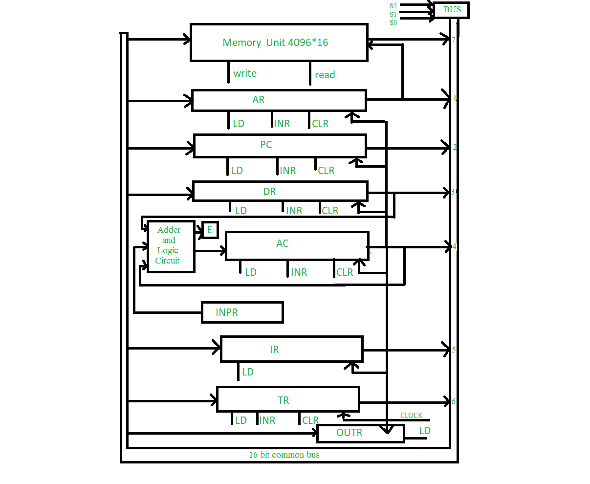
(b) What is the need of common bus? Draw common bus cycle.
Generally, computers use many registers for different purposes. We need to transfer the data and instruction between these registers. So, To transfers the data between the registers, the common bus system is used .
is prime or not.
OR
(c) Write an assembly language program to find factorial of the given
number.
1. Control Memory : The control memory consists of microprograms that are fixed and cannot be modified frequently. They contain microinstructions that specify the internal control signals required to execute register micro-operations. The machine instructions generate a chain of microinstructions in the control memory
2. Control Word : Control word is defined as a word whose individual bits represent the various control signal. The control words related to an instruction that is stored in microprogram memory. It is a set of micro-instructions in a micro-routine. In control words, microoperations are specified, they are known as microinstructions.
3. Control Address Register : Contains the address of the next microinstruction to be executed.
(b) Draw the flowchart of first pass of the assembler and explain working
of the same.
- The binary translation is done during the second pass.
- To keep track of the location of instructions, the assembler uses a memory word called a location counter (abbreviated LC).
- The content of LC stores the value of the memory location assigned to the instruction or operand presently being processed.
- The ORG pseudo instruction initializes the location counter to the value of the first location.
- Since instructions are stored in sequential locations, the content of LC is incremented by 1 after processing each line of code.
- To avoid ambiguity in case ORG is missing, the assembler sets the location counter to 0 initially.
- The tasks performed by the assembler during the first pass are described in the flowchart of figure.
- LC is initially set to 0.
- A line of symbolic code is analyzed to determine if it has a label (by the presence of a comma).
- If the line of code has no label, the assembler checks the symbol in the instruction field.
- If it contains an ORG pseudo instruction, the assembler sets LC to the number that follows ORG and goes back to process the next line.
- If the line has an END pseudo instruction, the assembler terminates the first pass and goes to the second pass.
- If the line of code contains a label, it is stored in the address symbol table together with its binary equivalent number specified by the content of LC Nothing is stored in the table if no label is encountered.
- LC is then incremented by 1 and a new line of code is processed.

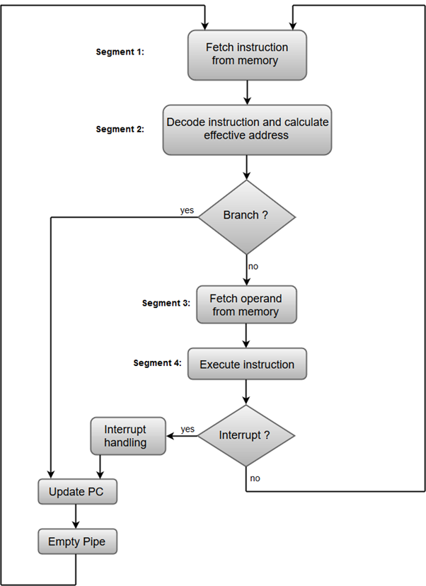
(c) What is the significance of pipelining in computer architecture? Write
a note on instruction pipeline.
Pipelining : Pipelining is a process of arrangement of hardware elements of the CPU such that its overall performance is increased. Simultaneous execution of more than one instruction takes place in a pipelined processor.
Thus, pipelined operation increases the efficiency of a system.
- Fetch instruction from memory.
- Decode the instruction.
- Calculate the effective address.
- Fetch the operands from memory.
- Execute the instruction.
- Store the result in the proper place.
Addressing sequence is able to increment the CAR (Control address register). It provides the facility for subroutine calls and returns. A mappings process is provided by the addressing sequence from the instructions bits to a control memory address.
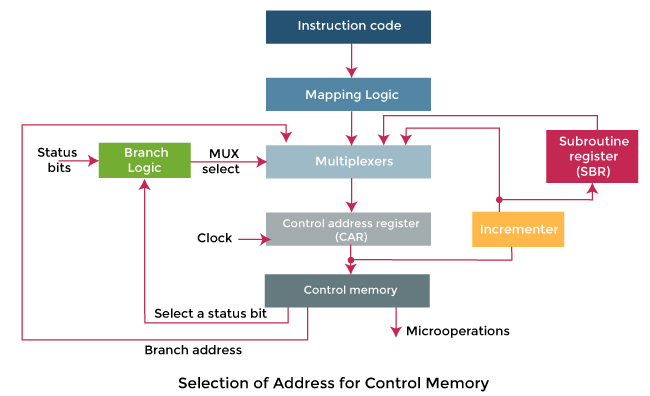
In the above diagram, we can see a block diagram of a control memory and associative hardware, which is required for selecting the address of next microinstruction. The microinstruction is used to contain a set of bits in the control memory. With the help of some bits, we are able to start the micro-operations in a computer register. The remaining bits of microinstruction are used to specify the method by which we are able to obtain the next address.
In this diagram, we can also see that the control address register are able to recover their address with the help of four different directions. The CAR is incremented with the help of incrementer and then chooses the next instruction. The branching address will be determined in the multiple fields of microinstruction so that they can provide results in branching.
If there are status bits of microinstruction and we want to apply conditions on them, in this case, we can use conditional branching. An external address can be shared with the help of a mapping logic circuit. The return address will be saved by a special register. This saved address will be helpful when the micro-program requires returning from the subroutine. At that time, it requires the value from the unique register.
An addressing mode specifies how to calculate the effective memory address of an operand by using information held in registers and/or constants contained within a machine instruction or elsewhere.
- The operator or opcode which determines what will be done
- The operands which define the data to be used in the operation
1. Direct Addressing Mode:
In direct addressing mode, the address field contains the address of the operand.
Effective Address (EA) = address field of operand 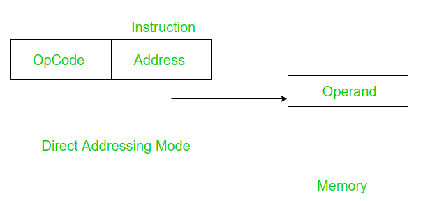
Example: Add the contents of register 1001 to the accumulator.
Add (1001) Only a single memory reference is required to access data. So no additional calculations are required to work out effective address.
2. Immediate Addressing Mode:
In immediate addressing mode, the operand is a part of the instruction.
Here the Operand = Address Field 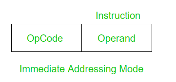
Example: Add 5 to the accumulator.
ADD 5 No memory reference is required to fetch data. So no additional calculations are required to work out the effective address. It is a fast method. But the downside is that it has a limited range.
3. Register mode: In register addressing the operand is placed in one of 8 bit or 16 bit general purpose registers. The data is in the register that is specified by the instruction.
Here one register reference is required to access the data.
Example: MOV AX,CX (move the contents of CX register to AX register)
Reduction Instruction Set Computer (RISC) is a multiprocessor particularly designed to process limited computer instructions in order to operate at a much higher speed. On any given system, there are many programs and many instructions being executed. It was discovered that only 10% of all instructions were frequently executed, and that the other 90% clogged the pipeline, thus contributing to the system slowness.
- inside the instruction, or
- in the register.
(b) Write a program to evaluate X = (a*b)/c+d in two address and three
address instruction formats.
(c) Draw neat and clean flowchart for divide operation. Explain with
example.
Q.4 (a) Differentiate isolated I/O and memory mapped I/O.
| Sr.No. | Isolated I/O | Mapped I/O |
|---|---|---|
| 1 | Memory and I/O have separate address space | Both have same address space |
| 2 | All address can be used by the memory | Due to addition of I/O addressable memory become less for memory |
| 3 | Separate instruction control read and write operation in I/O and Memory | Same instructions can control both I/O and Memory |
| 4 | In this I/O address are called ports. | Normal memory address are for both. |
| 5 | More efficient due to separate buses | Lesser efficient |
| 6 | Larger in size due to more buses | Smaller in size. |
| 7 | It is complex due to separate separate logic is used to control both. | Simpler logic is used as I/O is also treated as memory only. |
(b) Describe pipeline conflicts.
These conflicts arise when the instruction in the pipeline depends on the result of the previous instructions and these instructions are still in pipeline and are not executed yet.This problem generally occurs in instruction processing where different instructions have different operand requirements and thus different processing time.
(c) What is cache memory address mapping? Compare and contrast direct address mapping and set-associative address mapping.
Cache mapping refers to a technique using which the content present in the main memory is brought into the memory of the cache. Three distinct types of mapping are used for cache memory mapping.Here is a diagram that illustrates the actual process of mapping:

Example :
- Consider cache memory is divided into ‘n’ number of lines.
- Then, block ‘j’ of main memory can map to line number (j mod n) only of the cache.

2. Fully Associative Mapping-
In fully associative mapping,
- A block of main memory can map to any line of the cache that is freely available at that moment.
- This makes fully associative mapping more flexible than direct mapping.
Example- Consider the following scenario-
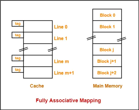
Here,
- All the lines of cache are freely available.
- Thus, any block of main memory can map to any line of the cache.
- Had all the cache lines been occupied, then one of the existing blocks will have to be replaced.
3. K-way Set Associative Mapping
In k-way set associative mapping,
- Cache lines are grouped into sets where each set contains k number of lines.
- A particular block of main memory can map to only one particular set of the cache.
- However, within that set, the memory block can map any cache line that is freely available.
- The set of the cache to which a particular block of the main memory can map is given by-
Cache set number = ( Main Memory Block Address ) Modulo (Number of sets in Cache)
Example- Consider the following example of 2-way set associative mapping-

Here,
- k = 2 suggests that each set contains two cache lines.
- Since cache contains 6 lines, so number of sets in the cache = 6 / 2 = 3 sets.
- Block ‘j’ of main memory can map to set number (j mod 3) only of the cache.
- Within that set, block ‘j’ can map to any cache line that is freely available at that moment.
- If all the cache lines are occupied, then one of the existing blocks will have to be replaced.
Virtual memory is important for improving system performance, multitasking and using large programs. However, users should not overly rely on virtual memory, since it is considerably slower than RAM. If the OS has to swap data between virtual memory and RAM too often, the computer will begin to slow down -- this is called thrashing.
- Allocating memory is easy and cheap
- Eliminates external fragmentation
- Data (page frames) can be scattered all over PM
- Pages are mapped appropriately anyway
- Large programs can be written, as virtual space available is huge compared to physical memory.
- Less I/O required, leads to faster and easy swapping of processes.
- More physical memory available, as programs are stored on virtual memory, so they occupy very less space on actual physical memory.
- More efficient swapping
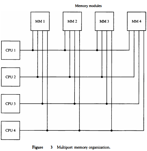
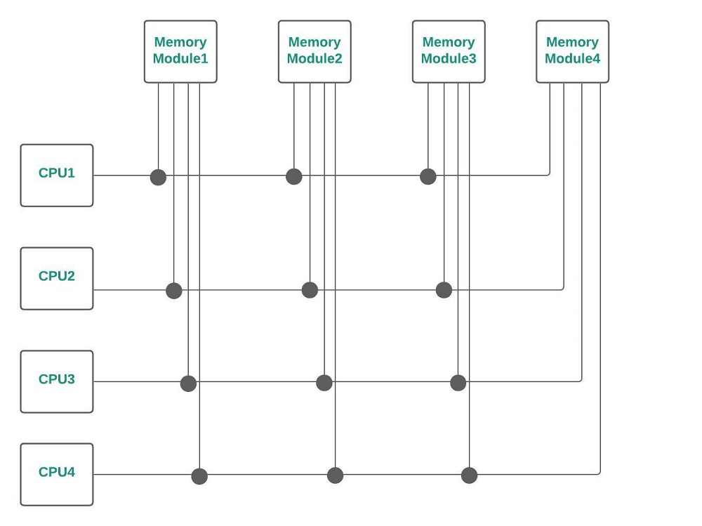
A multiport memory system employs separate buses between each memory module and each CPU.
This is shown in Fig . 3 for four CPUs and four memory modules (MMs).
Each processor busis Connected to each memory module.
A processor bus consists of the address, data, and control lines required to communicate with memory.
The memory module is said to have four ports and each port accommodates one of the buses. The module must have internal control logic to determine which port will have access to memory at any given time. Memory access conflicts are resolved by assigning fixed priorities to each memory port.
The priority for memory acoess associated with each processor may be established by the physical port position that its bus occupies in each module.
Thus CPU 1 will have priority over CPU 2, CPU 2 will have priority over CPU 3, and CPU 4 will have the lowest priority.
The advantage of the multi port memory organization is the high transfer rate that can be achieved because of the multiple paths between processors and memory.
The disadvantage is that it requires expensive memory control logic and a large number of cables and connectors. As a consequence, this interconnection structure is usually appropriate for systems with a small number of processors.
Cross bar Switch :
A point is reached at which there is a separate path available for each memory module, if the number of buses in common bus system is increased. Crossbar Switch (for multiprocessors) provides a separate path for each module.
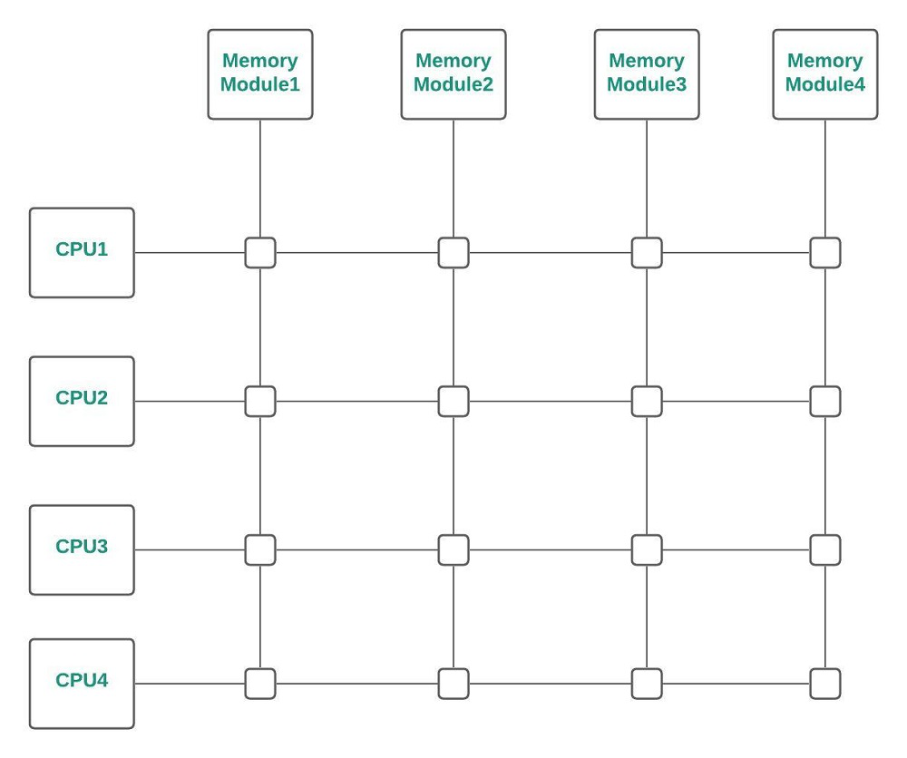
Cross-Bar Switch
Multiport Memory :
In Multiport Memory systems, the control, switching & priority arbitration logic are distributed throughout the crossbar switch matrix which is distributed at the interfaces to the memory modules.
Cache coherence : In a multiprocessor system, data inconsistency may occur among adjacent levels or within the same level of the memory hierarchy. In a shared memory multiprocessor with a separate cache memory for each processor, it is possible to have many copies of any one instruction operand: one copy in the main memory and one in each cache memory. When one copy of an operand is changed, the other copies of the operand must be changed also.
Example : Cache and the main memory may have inconsistent copies of the same object.
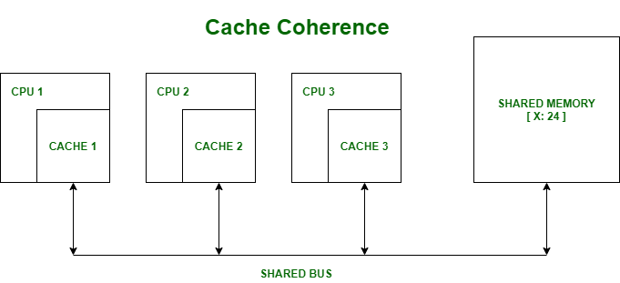
Suppose there are three processors, each having cache. Suppose the following scenario:-
- Processor 1 read X : obtains 24 from the memory and caches it.
- Processor 2 read X : obtains 24 from memory and caches it.
- Again, processor 1 writes as X : 64, Its locally cached copy is updated. Now, processor 3 reads X, what value should it get?
- Memory and processor 2 thinks it is 24 and processor 1 thinks it is 64.
As multiple processors operate in parallel, and independently multiple caches may possess different copies of the same memory block, this creates a cache coherence problem.
Data:
1 W = 4 B (word length is 32 bits)Physical address space (PS) = 4 G B = 230 W
Cache size (CS) = =16 KB = 214 B = 212 W
Block size (BS) = 8 W = 23 W
set associativity = 4
Formula:
number of bits = ⌈log2 n⌉
Number of lines in cache =
Number of sets in cache =
PAS = tag + set + block offset .....(in bits)
Calculation:
Number of lines in cache
Number of sets in cache = 29/4
Tag | Set | Block Offset |
x bits | 7 bits | 3 bits |
30 = x + 7 + 3
x = 20
∴ tag = 20 bits
The number of bits for the TAG field is 20.