Digital Fundamental Question And Answers-(Lets Crack The Exam)
1. State and explain
De Morgan’s theorems with truth tables.
- Module No. 1| (4M)
1.De Morgan's
First Theorem:-
Statement - The complement of a logical sum equals the
logical product of the complements.
Logic equation
- A+B¯=A¯.B¯A+B¯=A¯.B¯
Proof -

NOR gate is equivalent to bubbled AND gate.
2.De Morgan's Second Theorem:-
Statement - The
complement of a logical product equals the logical sum of the complements.
Logic equation
- A.B¯=A¯+B¯A.B¯=A¯+B¯
Proof -

NAND gate is equivalent to bubbled OR gate.
Truth Table to
prove De Morgan's Theorem:-

2. Implement AND, OR,
& EX-OR gates using NAND & NOR gates.- Module No. 1| (7M)


Implementation of EXOR Gate using
Universal gates.
a) Using NAND Gates


3. What is the race
condition in JK flip-flop? - Module No. 3| (3M)
Race Around
Condition in JK Flip-flop:
·
For J-K flip-flop, if J=K=1, and if clk=1 for a long period
of time, then output Q will toggle as long as CLK remains high which makes the
output unstable or uncertain.
·
This is called a race around condition in J-K flip-flop.
·
We can overcome this problem by making the clock =1 for
very less duration.
·
The circuit used to overcome race around conditions is
called the Master Slave JK flip flop.
Master Slave JK
flip flop:
·
Here two JK flip flops are connected in series.
·
The first JK flip flop is called the “master” and
the other is a “slave”.
·
The output from the master is connected to the two inputs
of the slave whose output is fed back to inputs of the master.
·
The circuit also has an inverter other than the two flip
flops.
·
The Clock Pulse and inverter are connected because of which
the flip flops get an inverted clock pulse.
·
In other words, if CP=0 for a master flip-flop, then CP=1
for a slave flip-flop and vice versa.

4. Design 1 - bit
Magnitude Comparator. - Module No. 3|
(4M)
A Comparator is
a combinational circuit that gives output in terms of A>B, A<B,
and A=B. This is entirely expected from the name. A digital comparator’s
purpose is to compare numbers and represent their relationship with each other.
A 1-bit comparator compares two
single bits.


5. Explain following
terms w.r.t Digital Logic Family.Module No. 1| (3M)
1.Propogation
delay :
The output of a logic gate does not change its state
instantaneously in response to the change in the state of its input.
There is a time delay between these two events ,which is
called as the propogation delay . Thus propogation delay is defined as time
delay between the instant application of an input pulse and the instant of
occurrence of the corresponding output pulse
2.Fan-in:
Fan-in is defined as the number of input gate has. For
example, a two input gate will have a fan-in equal to 2.
3.Fan Out :
Fan out is defined as the maximum number of the inputs of
the same IC family that a gate can drive without falling outside the specified
voltage limits.
Higher the fan out higher is the current supplying capacity
of the gate.
4.Power dissipation
:
Power dissipation is the amount of power drawn by the IC
due to the current flowing current through the IC as a result of the applied
voltage.
5.Figure of
merit :
The figure of merit of a logic family is the product of
power dissipation and propogation delay . It is called as speed power product .
The speed is specified in seconds and power is specified in W . The figure of
merit should be as low as possible .
The figure of merit is always a compromise between speed
and power dissipation . This means if we reduce the propogation delay then the
power dissipation will increase and vice - versa.
Figure of merit is always used as a common means for
measuring and comparing the over all performance of different IC families.
6.Noise Margin
:
Noise immunity is defined as the ability of logic circuit
to tolerate the noise without causing any unwanted changes in the output.
A quantitative measure of noise immunity is called as noise
margin.
6. Express the
Boolean function F = A + B’C in a sum of minterms. - Module No. 1| (3M)
Let,A = A(B + B’) = AB + AB’
This function is still missing one variable, so
A = AB(C + C’) + AB'(C + C’) = ABC + ABC’+ AB’C + AB’C’
The second term B’C is missing one variable; hence,
Let,B’C = B’C(A + A’) = AB’C + A’B’C
Combining all terms, we have
F = A + B’C = ABC + ABC’ + AB’C + AB’C’ + AB’C + A’B’C
But AB’C appears twice, and
according to theorem 1 (x + x = x), it is possible to
remove one of those occurrences. Rearranging the minterms in ascending order,
we finally obtain
F = A’B’C + AB’C’ + AB’C + ABC’ + ABC
= m1 + m4 + m5 + m6 + m7
SOP is represented as Sigma(1, 4, 5, 6, 7)
7. Reduce the
expression F = A [ B + C’ (AB + AC’)’]
- Module No. 1| (4M)
8. Simplify the
following Boolean function by using the tabulation method. F (A, B, C, D) = Σ m
(0, 1, 2, 8, 10, 11, 14, 15) - Module
No. 1| (7M)
9. Using D & E as
the MEV, Reduce F = A’B’C’ + A’B’CD + A’BCE’ + A’BC’E + AB’C + ABC + ABC’D’. -
Module No. 1| (7M)
10. Simplify the
Boolean function F (w, x, y, z) = Σ m (0, 1, 2, 4, 5, 6, 8, 9, 12, 13, 14)-
Module No. 1| (3M)
11. Design a full
adder and realize full adder using 3X8 Decoder and 2 OR gates.- Module No. 2|
(7M)
The truth table of a full adder is shown in Table1

i. The A, B and Cin inputs are applied to 3:8 decoder as an
input.
ii. The outputs of decoder m1, m2, m4 and m7 are applied to
OR gate as shown in figure to obtain the sum output.
iii. Similarly outputs m3, m5, m6 and m7 are applied to
another OR gate to obtain the carry output.
iv. Implement of full adder is shown in figure1.

12. Simplify the
Boolean function F = A’B’C’ + B’CD’ + A’BCD’ + AB’C’ - Module No. 1| (3M)

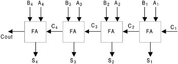
13. Explain 4 – bit
parallel adder. - Module No. 3| (4M)
Consider the example that two 4-bit binary numbers B 4B 3B 2B 1 and
A 4A 3A 2A 1 are
to be added with a carry input C 1. This can be done by
cascading four full adder circuits as shown in Figure 5.48. The least
significant bits A 1, B 1, and C 1 are
added to the produce sum output S 1 and carry output
C 2. Carry output C 2 is then added to the
next significant bits A 2 and B 2 producing
sum output S 2 and carry output C 3.
C 3 is then added to A 3 and B 3 and
so on. Thus finally producing the four-bit sum output S 4S 3S 2S 1 and
final carry output Cout. Such type of four-bit binary adder is commercially
available in an IC package.
14. Implement the
following function using 8X1 MUX F (A, B, C, D) = Σ m (0, 1, 3, 4, 8, 9, 15) -
Module No. 2| (7M)
- Implement of 8:1 mux

- Multiplexer (8:1mux)

15. Explain SR
flip-flop using characteristic table & characteristic equation.- Module No.
3| (3M)

Logic Symbol- The logic
symbol for SR Flip Flop is as shown below-

Truth Table-

Draw a k map using the above truth table-

=> Qn+1 = S + QnR’